Professional PCB-Mount Transformer Manufacturer — Custom High-Frequency Magnetics for SMPS & Electronics
High-efficiency ferrite transformers, inductors, and chokes engineered for PCB assembly — through-hole and SMD, safety-compliant, low loss, low leakage, and production-ready.
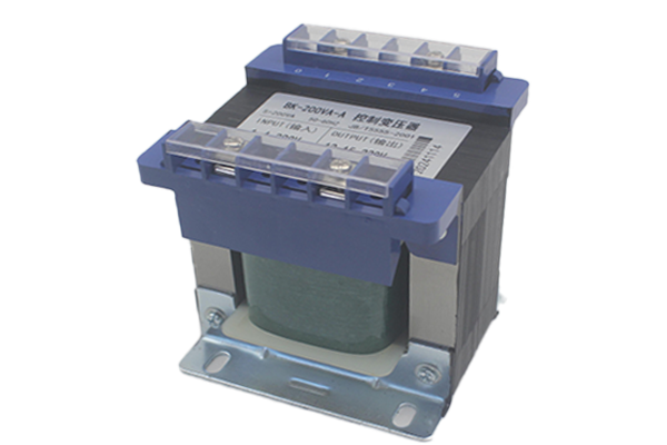
Professional PCB‑Mount Transformer Manufacturer — Custom PCB TRANSFORMER for SMPS & Electronics
Our custom PCB transformer solutions.High‑efficiency ferrite transformers, inductors, chokes, and pulse magnetics engineered for PCB assembly — through‑hole and SMD, safety‑compliant, low loss, low leakage, production‑ready with fast lead time.
Introduction to PCB‑Mount Transformer Manufacturing
PCB‑mount transformers are the core energy‑transfer elements inside modern power electronics — from chargers and adapters to LED drivers,
industrial controllers, networking gear and medical instruments. Unlike utility‑scale transformers that operate at 50/60 Hz,
PCB magnetics work at tens or hundreds of kilohertz, enabling smaller core sizes, tighter regulation, and higher efficiency when designed correctly.
They also shoulder multiple roles at once: isolation, conversion, signal coupling, common‑mode suppression, and noise shaping for EMI compliance.
A dedicated PCB‑mount transformer manufacturer aligns magnetic physics with manufacturability so your product passes safety and EMC the first time,
assembles repeatably on SMT/THD lines, and scales from prototypes to mass production without surprises.
Our team focuses on practical, test‑driven magnetics: choosing the right core set (EE/EF/EI/ER/EFD/ETD/EC/RM/PQ/EP/planar),
setting the air gap for target AL, crafting interleaved windings to balance leakage vs. capacitance,
specifying litz/foil/triple‑insulated wire to reduce AC resistance and meet insulation classes, and selecting varnish or potting systems to stabilize thermals and acoustics.
The result is a transformer that fits your PCB footprint, hits efficiency/ripple/thermal goals, and survives the field.
Transformer & Magnetic Components Portfolio
We design and manufacture a complete portfolio of PCB magnetics to support your SMPS and signal chains:
- High‑frequency power transformers for flyback, forward, push‑pull, half/full‑bridge and LLC resonant topologies (1–1000 W typical).
- Gate‑drive transformers for isolated MOSFET/IGBT control with low interwinding capacitance and excellent balance.
- Current transformers (CT) for primary current sensing with precise turns ratio and low phase error.
- Pulse transformers / PoE magnetics meeting IEEE 802.3 isolation & signal integrity requirements.
- Common‑mode chokes & EMI inductors tuned leakage and bias behavior to hit CISPR/EN emissions.
- PFC & output inductors with gapped ferrites, distributed‑gap powders or sendust for controlled saturation.
Form factors include through‑hole bobbins and SMD packages (tape‑and‑reel per EIA‑481), plus ultra‑low‑profile planar solutions using copper leadframes or PCB windings.
Design Principles for PCB Transformers
High‑frequency magnetics succeed when electromagnetic principles and factory discipline meet. Our core design principles:
- Topology‑aware design: Flyback benefits from controlled leakage for clamp networks, while LLC requires tight coupling and minimal stray capacitance. Forward needs balanced reset and proper window utilization; bridge converters prioritize copper fill and thermal paths.
- Air‑gap strategy: We set AL via center‑leg grind or shim, distributing gaps to minimize audible noise and fringing losses in adjacent copper. For inductors, we consider core material (ferrite vs powder) to manage bias and saturation gracefully.
- Winding methods: Layer, interleave and sandwich approaches are used to tune leakage and capacitance. Litz or foil mitigates skin/proximity effects at high frequency and current. Edge rounding and insulation interleaves avoid hot spots.
- Isolation & safety: Reinforced/double insulation via triple‑insulated wire (TIW) or margin tape barriers. Creepage/clearance are computed per IEC 62368‑1/61558 with pollution degree and over‑voltage category taken into account.
- Thermal management: Copper and core loss budgets are modeled; varnish impregnation or vacuum potting stabilizes windings and improves heat transfer. We evaluate temperature rise in chambers and align with your derating policy.
- EMI readiness: We bias interwinding capacitance and choke characteristics to ease conducted/radiated limits. Early pre‑scan sample support shortens your certification cycle.
Materials & Insulation Systems
Core Materials
We select Mn‑Zn/Ni‑Zn ferrite grades to balance loss vs. frequency and temperature stability. For inductors requiring bias tolerance, powdered iron, sendust or ferrite with distributed air gaps are applied. Planar cores enable thin profiles in height‑constrained products.
Conductors
Litz bundles reduce AC resistance above ~100 kHz; foil windings improve window utilization for high current rails. Primary/secondary segregation and shield windings manage capacitance and common‑mode noise.
Insulation Systems
UL‑recognized systems (Class B/F/H) using polyimide/polyester/PTFE tapes, TIW, and V‑0 plastics ensure dielectric strength and longevity. We supply full material declarations (RoHS/REACH) and can reference UL yellow cards on request.
Manufacturing Process — From Spec to Scale
1) DFM & Specification
We capture Vin range, Vout rails, power, frequency, isolation class, creepage/clearance targets, PCB footprint, pick‑and‑place constraints, and EMC goals. Our proposal includes core set, gap method, turns calculation, wire gauges, interleaving plan, loss estimate, and preliminary drawings.
2) Prototyping & Iteration
Samples are wound on pilot fixtures; AL is set; inductance, DCR, leakage and capacitance are measured; Hi‑Pot is validated. We iterate to hit efficiency, temperature rise and EMI objectives, providing data sheets and test logs.
3) Tooling & Pre‑Production
Bobbins/fixtures are tooled for repeatability; SMD versions get coplanarity verification and tray/embossed‑tape design (EIA‑481). Work instructions, control plans and AQL sampling are defined for PVT.
4) Mass Production
SPC monitors winding and solder processes; impregnation/potting viscosity and cure profiles are controlled. 100% electrical tests plus visual/AOI checks ensure stability; traceability ties lots to materials and results.
Testing, Reliability & Quality Assurance
Each batch undergoes a comprehensive validation matrix aligned to your risk profile:
- Electrical: primary/secondary inductance, leakage, DCR, turns ratio, interwinding capacitance, core loss estimation, saturation margin.
- Safety: Hi‑Pot (AC/DC per spec), insulation resistance, creepage/clearance audit, pin pull strength for THD/SMD variants.
- Reliability: temperature rise at rated load, thermal cycling, humidity soak, vibration/fixture robustness, varnish/potting adhesion tests.
- EMI readiness: sample pre‑scans, CMRR checks for chokes, shield effectiveness assessments.
Deliverables include test reports, CoC, and per‑lot records. On request we provide PFMEA/Control Plan and 8D for any non‑conformance.
Standards, Safety & Environmental Compliance
We support safety and environmental compliance for IT/AV, industrial, household and selected medical scopes:
- Safety: IEC 62368‑1, IEC 61558‑1/‑2‑16; UL recognition of insulation systems; flammability per UL 94 V‑0.
- EMC support: design for conducted/radiated emission limits; advice on Y‑capacitors, shields, choke selection.
- Environmental: RoHS, REACH (SVHC), halogen‑free upon request; full material declarations.
Customization Options, MOQ & Lead Time
Every application differs. We customize:
- Core set & footprint to fit PCB constraints (through‑hole, SMD, planar).
- Leakage & capacitance tuning to support snubbers, clamps, or resonant tanks.
- Thermal options: varnish, vacuum potting, heat‑spreader interfaces; target temperature rise defined.
- Markings, barcodes, private label; full traceability from materials to test results.
- Packaging for SMT (tape‑and‑reel) or wave solder (trays, tubes) with moisture protection.
Typical MOQ: 1k–3k pcs for custom designs. Lead times: samples 7–12 days; MP 3–5 weeks depending on BOM.
DFM/DFX Collaboration Tips
Early collaboration saves weeks on certification:
- Specify required creepage/clearance and insulation class; declare pollution degree and OVC.
- Reserve PCB keep‑outs for barriers if not using TIW; align pad design with solder process.
- Share thermal limits so we balance losses vs size; consider airflow and enclosure constraints.
- For SMT, confirm pick‑area, pocket depth and coplanarity; define drop test or vibration if portable.
- Set EMI targets; we will bias leakage/capacitance to ease compliance.
Industries & Applications
- SMPS & adapters: consumer chargers, industrial PSUs, instrumentation power.
- LED lighting: constant‑current drivers with low flicker and low ripple.
- Industrial & automation: PLCs, servo drives, sensors with robust isolation.
- Networking & PoE: Ethernet isolation, common‑mode suppression per IEEE 802.3.
- Medical/test: low leakage and special insulation options for sensitive devices (consult for 2 MOPP).
How to Choose the Right PCB Transformer Manufacturer
- Proven design library: ask for references near your topology and power level.
- Process capability: winding, gapping, impregnation/potting, SMT packaging and AOI controls.
- Documentation: full drawings, test plans, per‑lot reports; PFMEA/CP on request.
- Support: quick sampling, failure analysis, and on‑site/remote engineering until certification passes.
Share your spec (Vin, Vout, Pout, frequency, isolation class, creepage/clearance, footprint). We will reply with loss estimates, temperature rise projections, preliminary drawings, and a sampling plan.
Talk to Our Magnetics Engineers
Need a compact SMD gate‑drive transformer, a rugged flyback transformer for industrial SMPS, or a tuned common‑mode choke to pass EMI? Our magnetics team can design, validate, and scale your solution. Contact us to review schematics, layout constraints, and certifications — we’ll help you ship a reliable, compliant product on schedule.